
Konzept eines amerikanischen Hybrid-Verstärkers von 1955
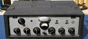
- Telefunken-Kino-Ton Verstärker 1951


- Grundig 1957 noch mit Röhren

- Loewe LO11 - Germanium Endstufe 1967 - 4 tubes, 13 semiconductors

von Gert Redlich im Aug. 2016 - Diese neumodischen Transistoren müssen doch für irgend etwas gut sein. Denn so richtigen Leidensdruck hatte damals niemand. Es gab ja bereits Kino-Röhrenverstärker mit 35 Watt Sinus und ELA-Verstärker mit 50 und 70 Watt Sinus von speziellen Herstellern. Damit gab es schon richtig Power - eben noch mit Röhren. Zuhause waren 10 Watt Sprechleistung in den fast 500.- DM teuren Edel-Röhren-Radios auch vollauf genügend. Also wofür diese Transistoren ?
Es kam aber die Zeit, als das mit den Autos und der Freizeit draußen im Grünen weltweit massentauglich wurde, in den USA zuerst und bei uns in Deutschland in der Regel 5 Jahre später, also nach 1960. Gleichzeitig brach ein "Run" nach mobilen "Kofferradios" aus, bei uns auch wieder 5 Jahre nach den USA. Und dort bei den Kofferradios gab es den echten Leidensdruck und zwar heftig. Denn die Röhren verbrauchten bei laut und leise nahezu gleich viel Strom. Im Auto hatten man(n) ja den dicken Starter-Akku, aber im Kofferradio ?
Beim mobilen Radio spielte das Gewicht eine recht große Rolle und damit war die Laufzeit über die Kapazität der Batterien begrenzt. Und jetzt endlich hatte man ein wirklich sinnvolles und verkaufbares Argument für Transistoren, die zumindest nach den Angaben der Entwickler in den Labors und damit auch der Verkäufer erheblich Strom sparen würden.
Die ersten Germanium-Transistoren von 1955
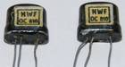
- absolut seltene DDR Typen

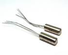
- Valvo Massenware

Die Entwicklung der Transistoren lag schon ein paar Jahre zurück. Und ein paar Enthusiasten entwickelten damit in den Laboratorien auch bereits sinnvolle Anwendungen. Doch massentauglich war das alles noch nicht, weil die ersten Germanuim-Transistoren noch in Handabeit für teures Geld hergestellt wurden. Die Qualitäten dieser ersten Transistoren waren aus heutiger Sicht sehr bescheiden. Daß die Entwicklung der Halbleitertechnik mal so rasant voranschreiten würde, auch mit Hilfe der Japaner, konnten sich nur wenige vorstellen. Wenn heute über 6 Millionen Transistoren auf einem Quadratzentimeter Platz finden, schaut fast keiner mehr hin. Aber damals war das absolute Utopie. Darum lesen Sie in den folgenden Kapiteln mal etwas über die erste(n) Transistorendstufe(n).
Interessant ist auch, wie auschweifend und ausführlich die Autoren das Thema behandelt hatten - damals im Juli 1955.
.
Class B Operation of Transistors (July-October 1955)

in a battery-operated portable amplifier - K. E. Loofbourrow
RCA - Tube Div., "Radio Corp. of America", Harrison, N. J.
Kapitel 1 - Chapter I - Design Considerations
CLASS B operation of transistors in the power-output stages of battery-operated portable amplifiers offers the important advantages of high collector-circuit efficiency, low standby idling current (and battery power), and a higher ratio of power output to collector dissipation per transistor than can be realized in class A operation. Because the rated power dissipation of many commercially available junction transistors is relatively low, the inherent high efficiency of class B operation is extremely attractive for many transistor applications.
There are 3 chapters

The characteristics of junction transistors and other design considerations for Class B operation are discussed in this article. Actual Class B audio amplifier circuits are extensively discussed and analyzed in the second part of this article.
In class B operation, the transistor is biased essentially at cutoff so that the output current is nearly zero when signal voltage is absent, and when signal voltage is applied, a current flows through the load in the output circuit during one half of the cycle.
"class B operation" - bei Röhren und Transistoren sehr ähnlich
In many respects, the advantages, limitations, and circuit requirements of class B operation are quite similar for both tubes and transistors. For example, low-impedance, well-regulated supply voltages are essential for optimum performance because of the high pulsating peak currents encountered in the output circuit.
If bias is employed, the bias supply should also be well regulated to prevent excessive distortion in the input-circuit voltages. Reasonable matching of tube or transistor characteristics is also required for satisfactory operation.
Der "Zwischenstufen-" (Treiber-) Transformator
When either tubes or transistors are used in class B, the driver stage must be capable of supplying the necessary peak input power and the power lost in the interstage transformer without excessive distortion.
.
Die "Kleinleistungs-" Verzerrungen
A major disadvantage of class B audio amplifiers is the relatively high value of odd-harmonic distortion that occurs at low power-output levels. This small-signal distortion, however, can be kept within allowable limits provided the transistor is designed for its optimum transfer characteristic and proper circuit-configuration and operation conditions are chosen.
.
Class B Circuit Advantages
In some respects, transistors differ from tubes when used in class B operation and display several advantages that make them somewhat easier and more desirable to use. For example, the lower impedance levels involved permit the use of smaller and less expensive interstage and output transformers.
In addition, the variation in input impedance with signal level is not nearly so great with transistors as with tubes when driven into the positive-grid-current region. As a result, design of the driver stage and driver transformer is simplified, and instability due to parasiticus is eliminated.
Because the output characteristics of junction transistors have extremely low-voltage, sharp "knees" in comparison with many vacuum tubes designed for class B operation, circuit designs having higher circuit efficiencies can be used which in some cases closely approach the maximum theoretical value of 78%.
Verstärker mit jetzt niedrigen Spannungen
When transistors have controlled large-signal characteristics, i.e., high-current amplification factors at values of high collector peak currents, it is possible to design power amplifiers that utilize very low supply voltages and yet maintain relatively high power sensitivity.
Large-signal "alpha" will be defined as the ratio of collector current to base current at a collector current of 50mA and a collector-to-emitter voltage of 1V. This measurement may be made for d-c or peak values with good correlation. Because the power gain or sensitivity of the transistor in large-signal amplifiers is proportional to this characteristic, high values of large-signal a are extremely desirable.
The peak-collector-current rating, which is determined for a given device by collector-saturation effects and life considerations, is conservatively selected for this transistor at 50mA.
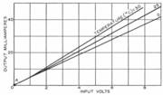
Die Verzerrungen in den Griff bekommen
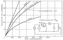
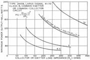
- Fig. 2. Typical large-signal current-amplification-factor characteristics for three junction transistors.

As shown in Fig. 2, the magnitude of "alpha" at a collector current of 50mA is approximately one-half that at low collector current. The non-linearity of the "alpha" characteristic, which is instrumental in determining the total harmonic distortion, can be altered by changes in the design or processing of transistors.
This nonlinearity is partially compensated for by the decrease in input impedance that occurs as the signal increases, causing more base current to flow for a given base voltage at high excitation levels. - A more ideal characteristic from the standpoint of a fall-off and reduced harmonic distortion is shown in the dashed curve of Fig. 2.
- Anmerkung : Die Grafik der Meßwerte zeigt die Größe des Basis-Stromes in Micro-Ampere zum Collectorstrom in Milli-Ampere, also die mögliche Stromverstärkung α "alpha" für verschiedene Transistor-Typen.
.
Transfer and Collector Characteristics
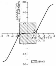
- Fig. 1a. The composite transfer characteristics for two 2NI09 junction transistors in Class B operation with a common emitter are shown at the top, left.

- Fig. 1b.The characteristics are modified at the bottom, left, to show use of projected-cutoff bias.

Composite transfer characteristics for two 2N109 transistors in class B operation are shown in Fig. 1.
Maximum collector-circuit efficiency is obtained when the base of each transistor is biased to cutoff so that the static operating collector current and the power dissipation are reduced to zero.
It is impractical to use zero bias in many circuits, however, because the nonlinearity in the small-signal region causes a high percentage of nonlinear distortion, especially at low levels.
At high values of output, the non-linearity in the curve causes progressively less distortion.
Über den Ruhestrom in der class b Endstufe
Cross-over distortion can be effectively reduced by the use of a small forward base bias, shown by point A in Fig. 1a, top, which allows a small quiescent collector current to flow during standby.
For any given transistor type, there is a particular value of base bias that results in a good balance between crossover distortion and collector-circuit efficiency.
A convenient method, for determining the operating point is to project the main part of the transfer-characteristic curve in a straight line to the cutoff point, as shown in Fig. 1.
The resulting composite curve is also shown in Fig. 1b, bottom. Use of projected-cutoff bias appreciably reduces cross-over distortion to a point at which any remaining distortion can be reduced by the use of negative feedback.
The change in the slope of the transfer characteristics at high values of base voltage is caused by the fall off in a or collector-current saturation.
.
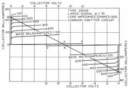
- Fig. 3. Composite collector characteristics for two 2N109 junction transistors.

The composite collector characteristics for two 2N109 transistors operating from a 9V supply are shown in Fig. 3.
Operation at point A on the load line BAC allows some quiescent collector current to flow at zero excitation voltage.
The reduction in the current amplification factor of the transistors at the higher values of collector current is illustrated by the compression of the collector characteristics in this region.
.
Ankoppelung der Endstufe an hohe Spannungen

- Transformator-Kopplung

When transistors are operated from high supply voltages, the maximum power output is limited by the maximum peak inverse collector voltage and the collector dissipation. When transformer coupling is used, the peak inverse voltage applied to each transistor is approximately twice the collector supply voltage. At lower supply voltages, the maximum power output is limited by the maximum permissible peak collector current and the collector dissipation.
Finding Operating Conditions
It is assumed that the input voltage is sinusoidal and that the transistors are biased at cutoff, and a one-volt "safe knee" is estimated, the following approximate formulas define the operating conditions - (Anmerkung : We will not show the formulas here, to old und no more interesting)
Transformer Requirements
The frequency response of junction-transistor class B amplifiers is determined primarily by the characteristics of the transformers and transistors used, although the exact relationships are somewhat complicated because of the intermittent collector currents present in the output circuit.
The low-frequency response is dependent upon the primary inductance of the transformers; the frequency at which the power output is 3db down from the output at mid-frequency is reached approximately when the primary reactance of the transformer is equal to the collector load impedance plus the total winding resistance of the transformers referred to the primary.
The high-frequency response is dependent upon the leakage reactance and winding capacitance of the transformers and the cutoff-frequency characteristic of the transistors. It is desirable that well balanced transformers be designed and that the leakage inductance between the two halves of the primary be minimized.
Balanced transformers minimize the d-c-polarizing currents, aid in the cancellation of even-order harmonics in the output, and reduce the possibility of distortion due to unbalance in the input signal.
Über den "output transformer"
Because high values of collector peak currents and low supply voltages are involved, the d-c resistance of the primary of the output transformer should be made as low as possible to retain high efficiencies.
The secondary winding of the driver transformer should also have low d-c resistance to minimize the effects of collector back currents upon the operating point. It should be emphasized that the transformer requirements mentioned are not particularly difficult to achieve because of the extremely low impedance levels involved.
Although there are circuit variations that make it possible to eliminate the output transformer, these circuits generally require the use of a power supply or a load impedance that is center-tapped. The driver transformer may also be eliminated in some circuits, although it is difficult in practice to obtain the relatively low d-c impedance required without the use of a transformer.
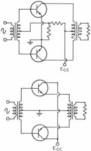
- Fig. I. Both the common-emitter Class B circuit at the top and the common-collector circuit at the bottom have base input.

Kapitel 2 - Chapter II - Basic Circuits
Several circuit configurations can be used to advantage in the design of large-signal junction-transistor audio amplifiers. Two of the most useful basic circuits are shown in Fig. 1.
Although the base-input, common-emitter circuit offers the highest power sensitivity, transistors used in this circuit must have fairly well-matched large-signal characteristics and relatively low values of collector back currents.
The average input resistance in this circuit is very low and is extremely nonlinear over the operating range. If the distortion requirements of the amplifier are severe, some negative feedback will be required.
Because the optimum bias voltage for minimum distortion varies with changes in temperature, the use of temperature-compensating elements such as diodes or thermistors in the bias supply is desirable.
The greatest practical advantage of the common-emitter circuit is its high power sensitivity.
.
Ein großes Problem : the temperature stability
The base-input, common-collector circuit, in which the load is in series with the emitter, has "built-in" d-c and a-c degeneration which greatly improves both the temperature stability and the distortion characteristics of the amplifier.
The input resistance in this circuit is relatively high and is more linear with excitation than that of the common-emitter circuit. As a result, high input voltages are required to develop the necessary driving power, the maximum value of which is limited by the supply voltage. This circuit accommodates a much wider variation in transistor characteristics than the common-emitter circuit, and does not require temperature compensation to correct for variations in collector reverse current.
The improved stability at higher temperatures and dissipations permits operation of a given transistor in the common-collector circuit at higher dissipation than in the common-emitter circuit. This circuit is also suitable for use with higher-power junction transistors. Because cross-over distortion is minimized without application of external base bias, better distortion performance is obtained at low power-output levels.
Considerable power sensitivity is sacrificed, however, for these improved characteristics, and it is necessary in many amplifier applications to add an additional driver stage.
Der Maximun Output ist nur noch abhängig vom Strom
- Fig. 2. Maximum power output is calculated by the expression shown in the upper left-hand corner of the chart.

When either of the basic circuits shown in Fig. 1 is used, the maximum power output is a function of the load impedance and supply voltage, as shown in Fig. 2.
Maximum power output is essentially independent of all transistor characteristics except the collector peak current capabilities. If the supply voltage is low, very low values of load impedance must be used to produce appreciable power output. The minimum value of load impedance is determined by the maximum peak-collector-current rating of the transistor.
As the supply voltage is increased, greater power output can be developed with the same load. If the common-emitter circuit is used, higher load impedances may be employed at higher supply voltages to provide the same maximum power output with a significant increase in power sensitivity.
Der Eingangswiderstand der class B Schaltung
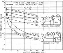
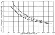
- Fig. 3. Input resistance vs. output current for two types of transistors in both common-collector and common-collector circuits.

- Fig. 4. Power gain characteristics of the two transistors considered in Fig. 3 in Class B push-pull circuits. For both circuits collector supply voltage is 9V, and signal is lOOO Hz.

The power sensitivity of junction-transistor class B amplifiers is a function of the input resistance, the load impedance, and the large-signal a of the transistors. Because the input resistance over the required operating range is not linear, the calculation or measurement of input resistance and power gain can be made most conveniently for peak values. The peak input resistance is equal to the peak input voltage divided by the peak base current. The peak power gain is equal to the peak power output divided by the peak input power.
Refferring to Fig. 3, in the common-emitter circuit, the peak input resistance is very nonlinear, increases with higher values of alpha and is independent of the low values of load impedance.
In the common-collector circuit, however, the input resistance is more linear and, for all practical purposes, is equal to the product of the load impedance and the peak current amplification factor.
Referring to the chart of Fig. 4, (right) the power gain of the common-emitter circuit depends to a large extent upon load impedance and large-signal current amplification factor.
The power gain of the common-collector circuit, however, is nearly independent of the load because the input resistance increases proportionally with the load. Because the power gain of the common-collector circuit is approximately equal to the peak current amplification factor of the transistors, the gain varies very little with changes in load impedance and only slightly for wide variations in large-signal a. The change in slope of the curves at low values of load is a result of the decrease in a at the resulting higher peak currents.
Das wichtigste Thema : Efficiency
The efficiency of either the common-emitter or the common-collector circuit has a maximum theoretical value of 78%. In practice, the actual efficiency depends upon the quiescent value of collector current, the supply voltage, the efficiency of the output transformer and the level of power output.
The efficiency of the two circuits is nearly the same for equal peak power output. In general, the choice of a high supply voltage results in slightly higher efficiencies because the "knee" voltage then becomes a smaller percentage of the total supply voltage. For example, the efficiency can be increased by 5 to 10% at rated output if supply voltage is increased from 4.5V to 9V.
Größte Effizienz bei Nennleistung

- Fig. 5. Characteristics of class B amplifier pairs having mismatched a and matched Rin.

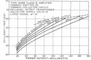
- Fig. 6. Efficiency decreases as power level is reduced.

- Temperature Effects


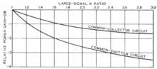
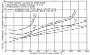
- Fig. 7. The common-emitter circuit has less distortion under each operating point.

The efficiency is greatest at full rated power output, and decreases as the power level is reduced, as illustrated in Fig. 6. For constant values of power output, the efficiency decreases for decreasing values of load. However, the efficiency at maximum power output increases as the load is decreased. It is possible, therefore, to design the amplifier with an optimum value of load impedance to give the required power output at maximum efficiency.
Low d-c primary resistance of the output transformer and tight coupling between the primary and secondary windings are required if the high efficiency is to be fully realized at the load. The variation in large-signal current amplification factor with matched or mis-matched transistors has no significant effect upon circuit efficiency because the maximum peak power is essentially unaffected by changes in large-signal a or mis-match in alpha. The variation in efficiency due to variations in alpha is only 2 to 3% at peak powers.
Distortion
Distortion in junction-transistor class B amplifiers is a function of the power output, the supply voltage, the input and load impedances, and the a characteristic of the transistors.
The effect of these factors is more severe in the common-emitter circuit, which employs no internal degeneration and, consequently, is more sensitive to circuit and characteristic variations.
The common-collector circuit has less distortion under each operating condition, as shown in Fig. 7, and shows the greatest significant improvement at low power-output levels, where cross-over distortion is effectively minimized without the use of external bias. For the common-emitter circuit, the curves show distortion at low power levels for the optimum value of bias.
Erstmals der Begriff des "hard clipping"
- Fig. 8. The class B circuits considered in this chart utilize 2NJ09 transistors operating with Ecc equal to 9V and at frequency of l.OOO Hz.

Distortion values would be considerably higher for this circuit (because of increased cross-over distortion) if the proper bias were not used. The change in the slope of the curves at high values of power output is due to "hard clipping", i.e., exceeding the point of maximum power as determined by the load impedance and supply voltage.
The increase in distortion as the load is decreased, as illustrated in Fig. 8, is caused primarily by the decrease in alpha of the transistor at the higher peak currents. A mis-match of 2 to 1 in the large-signal a characteristic results in about 2% additional distortion; a three-to-one mis-match causes approximately 5% additional distortion.
Der Gesamt-Klirrfaktor eines "class B amplifiers"
The over-all distortion of transistor class B amplifiers can be reduced, therefore, by the use of transistors that have well-matched large-signal characteristics, by an increase in the supply voltage and the load impedance, and by the use of negative feedback. The final amplifier should be designed to provide the desired balance between distortion and power sensitivity for the given application.
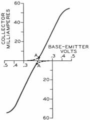
The transfer-characteristic curves shown in Fig. 1. illustrate the effects of ambient temperature upon transistors in common-emitter class B circuits. The operating point is designated by point A on the 25°C curve. If the common-emitter circuit is operated with a constant bias voltage, an increase in temperature causes an appreciable increase in quiescent output current and a consequent decrease in the maximum power output and output-circuit efficiency.
"cross-over distortion" bei niedrigen Temperaturen
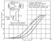
- Fig. 9. Temperature characteristics for the circuit enclosed in the chart.

- Fig. 10. Temperature characteristics for the circuit shown above.

- Fig. 10. Ecc equals 9v, the load impedence is 160 ohms, and the primary d-c resistance is 10 ohms.

A decrease in temperature reduces the quiescent collector current almost to zero, thereby increasing the maximum power output and the efficiency slightly, and introduces cross-over distortion because the transistor is then operating over the nonlinear portion of its transfer characteristic. For optimum performance in the common-emitter circuit over a wide temperature range, temperature-sensitive elements should be used in the bias network so that the bias voltage changes with temperature and the quiescent collector current remains constant.
This bias may be obtained conveniently by using a thermistor or germanium diode in a resistive network, as shown in Fig. 9, to provide a curve of network resistance vs temperature having a slope approximating that of the transistor characteristics over the required operating range.
In many applications, however, it is practical to use the common-emitter circuit over reasonable temperature ranges without the use of temperature compensation ii a higher operating point is selected with a slight sacrifice in efficiency.
The effect of temperature variation on the transfer characteristic for the common-collector circuit is shown in Fig. 10. Because the load impedance is in scries with the input signal in this circuit, high input voltages are required to drive the transistor to its rated peak current.
Der Betrieb fast ohne Ruhestrom
The curves of Fig. 10 are reasonably linear, even in the low-current regions. As a result, the transistors may be operated at zero bias without introducing the problems of low-level distortion at room temperature or with temperature variations. In this circuit, therefore, no bias supply or temperature-compensating network is required for optimum performance.
The shift of the curve with temperature at the high-current end of the scale causes a slight variation in the maximum power and the power sensitivity of the circuit. This variation may be reduced by the use of an output transformer having increased d-c primary resistance in series with the emitter load, resulting in increased d-c stability.
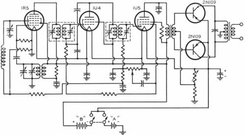
Kapitel 3 - Chapter III - Das Hybrid Radio
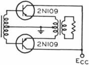
USING junction transistors in class B in hybrid receivers in place of a power output tube effect an increase in available power output and a substantial reduction in required battery power, as illustrated.
- Fig. I. Schematic of a hybrid radio with two transistors operating Class B push-pull in the output.

.
Ein Verbrauchs-Vergleich mit verschiedenen Batterien
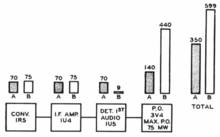
- Fig. 2a. Stage-by-stage battery power needs in milliwatts for an all-tube portable

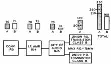
- Fig. 2a. .. and a hybrid radio below. Dotted lines indicate normal conditions. "A" and "B" stand for A and B batteries, respectfully.

Approximately 75% of the relativey expensive B-battery power and 40% of the less expensive A-battery power is consumed by the output stage. When transistors are used in the output stage of the receiver, a considerable saving in battery power can be obtained. It should be noted that the power for the transistor output stage is obtained from the A-battery supply.
- Anmerkung : Röhren-Kofferradios wurden sehr oft mit 2 Batterien betrieben, der Heizspannungsbatterie (irgendwo um die 6 bis 9 Volt und der Anodenspannungsbatterie mit fast 100 Volt.
The battery-drain value given for the receiver using transistors is higher than that which would occur in normal operation because the power consumed by the output stage in class B operation varies with the signal level. The value given represents continuous operation of the receiver at maximum power output under sine-wave conditions. Under conditions of normal speech and music, the average power consumption would be cut as shown.
.
Teils Röhren - Teils Transistoren
A circuit diagram of a part-tube, part-transistor battery-operated portable radio receiver is illustrated.
The tube filaments (die Heizdrähte in den Röhren), which originally were connected in parallel, are connected in series so that a common supply voltage can be used for the filaments and the transistors.
Consideration must be given in this circuit to the normal biasing arrangements required with series-string operation of tubes. The operating conditions of the pentode section of the first audio stage are modified to provide adequate driving power for the transistor output stage and to increase the over-all power sensitivity of the audio system.
Der Betrieb mit 45 Volt
The sensitivity of the resulting audio system is equivalent to that of receivers using a subminiature output tube and operating from a supply of 45V or less. This sensitivity is about 10db below the audio sensitivity of receivers using a miniature output tube similar to the 3V4 and operating from a supplv of 67V.
Wenn die Batterie zur Neige geht . . .
The sensitivity of all-tube receivers, however, generally decreases more rapidly with battery life than the sensitivity of the illustrated receiver. Consequently, any difference in performance between the two systems is reduced with battery life. In some existing receiver designs having an r-f stage, the loss in audio sensitivity is automatically compensated for by the r-f sensitivity, which is normally more than adequate.
In many other receivers, additional sensitivity may be gained by modification of the i-f stage, or by use of more sensitive antennas and higher efficiency speakers.
As compared to an all-tube receiver, therefore, the part-tube, part-transistor receiver has nearly equivalent audio sensitivity, similar distortion characteristics, equal or greater power output with a maximum value that is more nearly constant with battery life, and considerably higher over-all efficiency.
Zwei Wege für die Zukunft :
The greater battery efficiency can be used in either of two ways:
- (1) portable equipment can be designed to have extremely small size and light weight by the use of miniature batteries compatible in size with the low power requirements; or
- (2) portable equipment can be designed using conventional battery sizes resulting in substantial improvements in battery life and a sizable reduction in operating cost.
.
/hr.
.