
Die Transistoren waren 1953 brand neu - selbst für Ingenieure
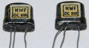
- absolut seltene DDR Typen

von Gert Redlich im Aug. 2016 - Und die ersten Germanium Transistoren waren sensibel und kritsch. Ein alter Entwickler - ein studierter Maschinenbauer - verriet mir, daß sie damals hunderte von den damals extrem teuren Transistoren "verheizt" hatten, bis sie endlich raus hatten, wie es NICHT ging. Nach diversen "Mahnungen" der Chefs, den "Laden" (der war im Schwarzwald, also nicht bei BRAUN in Frankfurt oder in Fürth) nicht zu ruinieren, wurde etwas vorsichtiger getestet. Und das alles, obwohl es von Siemens bereits frühe Musterschaltungen für kleinste Verstärker gab. Man mußte es dennoch ausprobieren, wo die damals sehr niedrigen Grenzen lagen.
In dem nachfolgenden Artikel von RCA vom Januar 1954 beschreiben die Autoren recht umfangreich, daß das mit der physikalischen Temperatur-Empfindlichkeit der Germanium Transistoren bei steigender Umgebungstemperatur überhaupt nicht trivial war.
.
Power Transistors for Audio Output Circuits


Reprinted from ELECTRONICS - January, 1954
By L. J. GIAGOLETTO - Radio Corporation of America
RCA Laboratories Division - Princeton, New Jersey
Analysis of operating characteristics of typical power transistors and influence of finite base-lead resistance, temperature, frequency, and generator resistance. Biasing problems for typical audio power output stages are also considered.
Introduction
Dependence of transistor characteristics on temperature presents a difficult problem to equipment designers, especially those involved in power circuit work where unavoidable internal power losses may be appreciable.
This article presents a method for analysis of transistor power amplifiers. For purposes of illustration, calculations have been carried out using a typical experimental power transistor. The method of calculation is developed generally so that circuit design using other junction transistor types can be readily carried out.
General Types
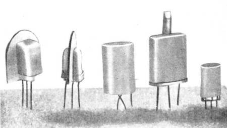
- Titelbild - Typical power junction transistors. Second from right and center transistors are discussed in text and shown in detail in Fig. 1. Unit on far right is small transistor encased in plastic; two on left have radiating fins connected to base and emitter.

The photograph shows several experimental power transistors *1).
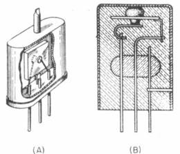
- FIG. 1 - Assembly details of liquid-cooled (A) and metallic-conduction cooled (B) power transistors

The liquid-filled enclosure, shown in detail in Fig. 1A, is a reasonably simple and effective method of construction. The transistor is fabricated by standard techniques and then encased in a liquid-filled metal shell. Heat generated by the transistor is transferred to the metal shell by the liquid coolant. Benzene, toluene, and xylene are suitable liquids. Toulene has proved the most successful due to its low viscosity and relatively high boiling point. In addition to the simple method of construction, the liquid-enclosed power transistors have been particularly attractive because the germanium junctions suffer very little deterioration.
The use of a liquid, particularly an inflammable liquid, is not a very satisfactory solution for most applications. Consequently, the method of construction shown in Fig. 1B was developed. Here, a large metal surface is soldered directly to the germanium assembly. Heat is transferred to the large metal surface by metallic conduction with very little drop in temperature. The metal surface may be soldered to any of the three transistor elements and then encased in plastic for mechanical and environmental protection. The sketch shows a metal cup soldered to the collector.
Maximum Dissipation
Heat transfer *2) can take place by radiation, conduction and convection. All three of these processes are potentially of importance in the removal of heat from a power transistor. Using heat transfer equations to calculate the effects of radiation, conduction and convection heat powers, the total heat power transfer for the cup power transistor previously mentioned is 1.28 watts for a 50-degree C temperature rise above a 25-degree ambient temperature. For these operating conditions, the cup power transistor can be rated as having a maximum power dissipation of approximately one watt.
This maximum power rating depends to a considerable extent upon the maximum permissable operating temperature, which has been arbitrarily picked at 75 C. The maximum permissable operating temperature will depend rather critically upon the changes in operating characteristics with temperature, an item to be considered subsequently, and upon life test data.
.
- Anmerkung : Auch hier werden die Temperaturen in Grad Celsius angegeben. Das war für die USA insbesondere damals sehr ungewöhnlich, da dort heute noch in Fahrenheit gemessen wird.
.
Shockley's analysis

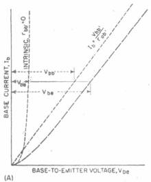
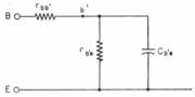
- FIG. 2 - Diagram shows intrinsic transistor together with extrinsic base-lead resistance found in practical units

The operation of a junction transistor has been analyzed *3). Careful measurements of small-signal junction transistors indicated that Shockley's analysis may be used for quantitative results if it is applied to an ideal intrinsic transistor. The actual transistor has certain extrinsic elements which must be added to the intrinsic transistor. A very important extrinsic element is a base-lead resistance, shown diagramatically in Fig. 2.
One of the basic assumptions of Shockley's analysis is that the minority carrier density is much smaller than the majority carrier density throughout the base region. This assumption is hardly satisfied by power transistors where the minority carrier density is generally many times the majority carrier density.
Nevertheless, as will be seen, many of the gross aspects of power-transistor characteristics are given by the Shockley analysis. In those cases where there is a considerable difference, use can be made of modified analyses *4) to determine the appropriate results.
According to Shockley's analysis, the d-c characteristics of a junction transistor are given by equations.
In these equations Ie and Ic are the emitter and collector d-c currents respectively and V eb and Vcb are the emitter-to-internal-base and collector-to-internal-base d-c voltages respectively. The four g's are d-c conductance coefficients which can be considered similar to the perveance coefficient employed in electron tube studies.
coefficients and parameters
These d-c conductance coefficients must not be confused with a-c conductance parameters although the coefficients can be measured *5) by the same means employed for measuring the a-c parameters when the d-c terminal voltages and currents are both zero.
.
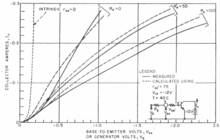
- FIG. 3 - Static transfer characteristics for power transistor

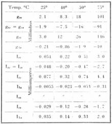
- Table I - Power Junction Transistor Coefficients and Saturation Currents

The Greek letter A is used in place of e/kT where e is the charge of an electron in coulombs, k is Boltzmann's constant in joules per degree K, and T is the operating temperature in degrees Kelvin (At room temperature, 27 C (300 K), A = -38.6 volts hoch -1 for electrons and +38.6 volts hoch -1 for holes.). *6)
Currents Ice and Ics are the emitter and collector saturation currents, respectively, and represent currents due to thermally-generated carriers in the base that flow to the emitter and collector when both are biased more than a few tenths of a volt in the reverse direction.
If the d-c conductance coefficients are known, the intrinsic-transistor characteristics can be readily,computed by means of formulars 5, 6 and 7 (formulars not shown here). This has been done for the collector current for a typical power transistor, and the results are shown by the dotted curve in Fig. 3.
The measured d-c conductance coefficients used in these calculations together with the corresponding d-c current coefficients and saturation currents are tabulated in Table I under the appropriate temperature heading of 40 C.
The dotted curve of Fig. 3 can be considered to be the intrinsic transfer characteristic of the transistor; that is, the transfer characteristic that would be obtainable if Rbb were zero.
current-amplification factor "alpha"
- Fig. 4-Construction of base characteristics (A)

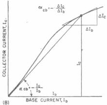
- and d-c and a-c collector-to-base current amplification factors (B)

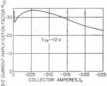
- Fig. 5-Amplification factor (d-c) as a function of collector current

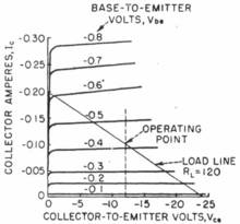
- Fig. 6-Output load characteristics

The graphical relationship between the intrinsic and actual base characteristic is shown in Fig. 4A. The actual base-to-emitter voltage is obtained by adding to the intrinsic voltage Vb'e the voltage drop Vbb' across the base-lead resistance. The latter voltage will generally be several times larger than the former, particularly at larger currents, so that the base characteristics will be essentially linear. That is the base current will be approximately linearily related to the base-to-emitter voltage.
Actual transfer characteristics can be obtained by a similar graphical construction with the use of the base characteristics. An alternate method of calculation is to use the relationship between collector current and the base current. This relationship can be expressed in terms of a d-c current-amplification factor "alpha" cb.
Figure 4B shows how the d-c and a-c collector-to-base current-amplification factors are related to the currents. As shown in Fig. 5, the d-c current-amplification factor decreases approximately hyperbolically at larger collector currents. This drop-off is an important aspect of power-transistor operation and can be explained by modified analyses. *4)
With the aid of Fig. 5 the actual transfer characteristics can be determined.
The transfer characteristics
The actual transfer characteristics determined by this manner are shown by the dashed curve labelled Rg=O in Fig. 3. For comparison purposes the measured transfer characteristics are shown by the corresponding solid line in the same figure.
Base-lead resistance can be measured directly by small-signal methods, but for the purposes described herein, it can best be determined by fitting a calculated characteristic to a measured characteristic.
The implication thus far has been that the base-lead resistance rbb' is independent of current. This is not exactly the case as rbb' will decrease somewhat as the collector current is increased.
This, in part, accounts for the discrepancy between the calculated and measured transfer characteristics of Fig. 3.
Most calculations on power transistors can best be carried out with the aid of the transfer characteristics. Occasionally the base and collector characteristics may be of interest.
The base characteristics as shown in Fig. 4A have already been considered. The collector characteristics for the power transistor under consideration are shown in Fig. 6. These curves will be employed subsequently in considering the optimum output loading of the transistor.
Frequency Characteristics
- FIG. 7-Input equivalent circuit for small-signal transistor operation

For small-signal operation the input equivalent circuit has the form shown in Fig. 7. The resistor marked rb'e represents the flow of carriers to the base and is reciprocally proportional to base current. For a power transistor operating at a collector current of 100mA, rb'c would be of the order of 10ohms.
Capacitor Cb'e represents the storage of charge carriers in the base region. Its value is directly proportional to the square of the base thickness and to emitter current. Accordingly the actual value of Cb'c will depend greatly upon the base thickness.
As an example, for a base thickness of 0.002 in. Cb'e would be of the order of 0.5 uf at a collector current of 100mA. On a small-signal basis, Cb'e will have a pronounced frequency effect.
For large-signal operation, rb'e and Cb'e will vary with the applied signal. It is this variation together with similar variations in other reactive elements that complicate even an approximate study of large-signal frequency characteristics.
Temperature Effects
Germanium is a semiconductor, and as such exhibits a pronounced temperature-resistivity variation *6). The relatively impure germanium customarily employed in transistors will generally exhibit an increase in resistivity with temperature at approximately room temperature. At higher temperatures the impure germanium decreases in resistivity with increasing temperature in the same manner as pure germanium.
The manner in which temperature enters into transistor operation can be ascertained with the aid of Eq. 11 and 12. The transistor characteristics will be affected by temperature variations due to a change in the value of A. In addition, the saturation currents and the current coefficients change rapidly with temperature.
If the saturation currents and current coefficients are known at one temperature, their values at some other temperature can be determined by applying a suitable temperature correction factor.
.
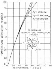
- FIG. 8-Curves for finding germanium temperature correction factor

For convenience, this temperature correction factor which is approximately the same for both n and p germanium normalized to room temperature of 25 C is given in Fig. 8. It is apparent from the values of the temperature correction factor that the saturation currents and current coefficients will change rapidly with temperature. The data in Table I exhibit this very rapid variation with temperature.
temperature variations
Fortunately, the actual transistor characteristics are not quite so sensitive to temperature changes. As temperature is increased, Ice and Ibe increase rapidly, but A decreases, and since A enters as a positive exponent some of the increase in Ice and Ibe is compensated. The temperature stability of a junction transistor is adversely affected by the presence of rbb'.
As the temperature is increased, base current decreases. The resulting change in voltage across rbb' is in such a direction as to further increase the collector current. The decrease in base current with increase in temperature is due to the presence of Ib2 in Eq. 13. Current Ib2 has a sign opposite of Ibe and its increase with temperature is uncompensated. Accordingly, as the temperature is increased, Ibs contributes a progressively larger share to Ib and may actually produce a reversal in the direction of Ib.
.
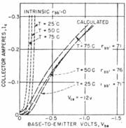
- FIG. 9-Change in static transfer characteristics with tempertaure

The manner in which the calculated transfer characteristics change with temperature is shown in Fig. 9. For these calculations, it was assumed that the transistor was made of 4 ohm-cm n-type germanium. Maximum resistivity of this material occurs at approximately 50 C, and the resistivities at 25 C and 75 C are about equal.
Audio Output Stage
In the design of an output stage the d-c power supply voltage is usually specified. Let this be 12 volts. Generally, the d-c supply voltage will be limited to about half the collector breakdown voltage.
The maximum power dissipation for the "cup" transistor has been determined to be 1.28 watts for a 50 C temperature rise above 25 C ambient. Thus, a static collector current of 100mA can be accommodated. For maximum power output an output resistance of 120 ohms is indicated. A resistance of this value is shown by the load line in Fig. 6. A maximum a-c power output of about 0.6 watt can be expected.
remember - we are talking about a 0,6 watt amp
Additional details concerning the output stage can be obtained by referring to the transfer characteristcs in Fig. 3. The transfer curve (solid curve marked Rg = 0) shows that a base-to-emitter bias voltage of -0.48 volt is required for the 100mA operating point.
A peak driving voltage of 0.76 - 0.48 = 0.28 volt is required. Since the input resistance will consist mostly of rbb' the a-c input power will be approximately 5.2 x 10 hoch -4 watt and the power gain 1,150 or 30.6 db. These calculations are approximate. With the aid of the transfer characteristics output distortion can be computed. *7)
The preceding calculations are based upon a zero resistance signal source. This will normally not be the case. The actual situation (RG > 0) is similar to a vacuum tube being driven into grid conduction resulting in increased distortion plus an increase in driving voltage required for full output. Frequency response also suffers from the presence of RG.
.
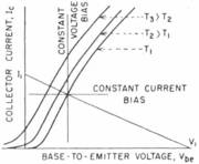
- FIG. 10-Curves show effect of changes in temperature on bias

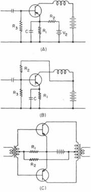
- FIG. 11-Bias arrangements for typical audio output power amplifiers

The circuit operation when RG > 0 can be determined by Thevenin's theorem, considering the source as a voltage generator VG in series with RG. In the transistor circuit Ra is in series with rbb and the two can be lumped together and considered part of the transistor. The result is a transistor with a larger effective rbb' being driven from a generator of zero internal resistance.
The transfer characteristics for the new transistor can be constructed in the same manner as already described. Figure 3 shows two transfer characteristics determined in this manner when RG = 50 and 100 ohms. The base-to-emitter voltage includes the voltage drop across RG and is therefore the generator voltage. The corresponding measured transfer characteristics are also shown.
To get satisfactory operation over a range of temperatures, the biasing of the output stage must be given careful attention.
Figure 10 indicates the change in the operating point with changes in temperature. For stability, constant-current bias has the most advantages even though it is more difficult and expensive to achieve. An absolute constant-current bias is not feasible; an intermediate bias condition is generally used.
Two methods of obtaining intermediate bias for class-A operation are shown in Fig. 11A and 11B. The biasing of a push-pull class-B stage is somewhat less complicated. A typical arrangement is shown in Fig. 11C. Since the base current will generally decrease as the temperature is increased (Fig. 9), the base bias with the circuit of Fig. 11C will tend to increase as the temperature is increased.
The net result of these two effects will be to cause the quiescent collector current to increase. This factor must be taken into account in designing the class-B stage to insure that operation remains within the maximum limitations of the transistor. One method of achieving stability is to use a temperature-sensitive resistor for R, or Rs.
Complementary symmetry circuits *9 and *10) provide numerous additional circuit possibilities for audio output stages using power transistors. For example, the relatively simple biasing requirements of the push-pull amplifier can be taken advantage of without addition of bulk and weight in the form of transformers.
.
References (January, 1954 - ELECTRONICS)
.
- (1) These units are the work of D. A. Jenny and L. D. Armstrong-, RCA Laboratories, Princeton, N. J.
- (2) William H. McAdams, "Heat Transmission," McGraw-Hill Book Co., New York.
- (3) W. Shockley, M. Sparks and G. K. Teal, P-N Junction Transistors, Phys Rev, p 151, July 1951.
- (4) W. M. Webster, On the Variation of Junction Transistor Current-Amplification Factor with Emitter Current, submitted for publication in Proc IRE.
- (5) L. J. Giacoletto, Bridges Measure Transistor Parameters, Electronics, p 144, Nov. 1953.
- (6) P. G. Herkart and J. Kurshan, Tbeoretical Resistivity and Hall Coefficient of Impure Germanium Near Room Temperature, RCA Rev, Sept. 1953.
- (7) P. E. Terman, "Radio Engineer's Handbook", p 380, McGraw-Hill Book Co., N. Y.
- (8) Stabilization method used by L. E. Barton of RCA Laboratories in a class-B output stage of portable personal receiver.
- (9) G. C. Sziklai, Symmetrical Properties of Transistors and Their Application, Proc IRE, p 717, June 1953.
- (10) R. D. Lohman, Complementary Symmetry Transistor Circuits, Electronics, p 140, Sept. 1953.
.