
Ein 10 Watt Transistor Verstärker - aber bereits vom Mai 1958 !!

von Gert Redlich im Aug. 2016 - Für uns Deutsche war natürlich Max Grundig der große Held, der uns die Transistoren schmackhaft zu machen versuchte. Das war natürlich Eigennutz von Grundig, denn die beiden Grundig Röhrenendstufen NF1 und NF2 wurden in den Grundig Musiktruhen - und nur für die waren die ja entwickelt worden - zu heiß, sie wurden viel zu viel zu heiß.
Auch wurde uns interessierten Jungspunden suggeriert, damals jedenfalls so um 1963 herum, als ich gerade mal 14 Jahre alt war, daß diese neumodischen Transistoren zwar in USA erfunden worden seien, doch die würden jetzt hier bei uns bei Siemens und Telefunken hergestellt - und auch bei TEKADE in Nürnberg - bereits seit 1956 !!
Das war natürlich auch viel Unsinn - auch hier bei uns im damals noch jungen Deutschland (West).
Das war also unser verkappter deutscher Lokalpatriotismus, übrigens genauso engstirnig wie in den USA, bei denen das Tonbandgerät selbstverständlich auch von der Firma Ampex aus Californien erfunden wurde. Doch beim Durchforsten der großen Stapel Dokumente aus den diversen Nachlässen kommen immer mehr Publikationen ans Licht, die eine ganz andere Sprache sprechen und die uns die Augen öffnen, jedenfalls mir.
In alten verschlissenen Kartons lagen sie, die "Preprints" (das sind Nachdrucke) von uralten "RCA" Publikationen

- Abholen fahren - und jedesmal ist das ganze Auto voll

RCA war einmal der Welt größter Elektronik Konzern, bevor er etwa 1984 von den sogenannten "Heuschrecken" (sogar von den eigenen Gesellschaftern) zerschlagen wurde. Und bei RCA in deren berühmten Labors in Princeton und Umgebung wurden weltbewegende Erfindungen gemacht oder vorhandene Erfindungen perfektioniert. So wurden mit den ersten brauchbaren Transistoren die Grundlagen für frühe Hifi-Verstärker erforscht, lange bevor bei den amerikanischen Firmen Harman Kardon oder The Fisher oder H.H. Scott oder anderen Mainstream Herstellern soetwas auf den Markt kam.
.
A Ten-Watt High-Quality Transistorized Audio Power Amplifier
February 1958 - ROBERT MINTON C. F. WHEATLEY - Radio Corporation of America
How To Use Transistors In The Design Of A High-quality, Audio-frequency Power Amplifier.
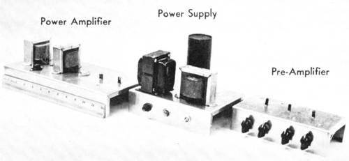
- Final Assembly: The Ten Watt Transistorized Amplifier

The transistor amplifier - absence of microphonics and hum
The dependability of transistors as amplifying devices has been demonstrated by their use in many types of electronic equipment. The addition of power transistors to the audio line completes the complement of transistors necessary for the design of a completely transistorized high-power, audio-frequency amplifier.
Beside small size, the most outstanding advantage gained from the use of transistors in such equipment is the absence of both microphonics and the hum associated with heater-cathode devices.
.
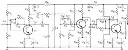
- Fig. 1a - Die Vorstufe (mit diversen Fehlern im Schaltplan)

The circuit shown in Fig. 1a represents one approach to the design of a high-quality transistor amplifier. This amplifier, consisting of seven amplifying stages, is capable of delivering 10 watts of output power with low harmonic and intermodulation distortion over a wide range of frequencies.
Beside these characteristics which are common to all good amplifiers, electrical measurements and a favorable reaction to listening tests indicate that this design yields a satisfactory high quality power amplifier.
.
Preamplifier Design Requirements
The preamplifier portion of Fig. 1b was designed to transmit a signal from a ceramic or crystal pickup into the power amplifier. The following objectives are considered in its design:
.
- 1. A frequency-corrective network to compensate for the recording characteristic of records.
- 2. An input impedance characteristic suitable for the pickup employed.
- 3. Continuously variable bases and treble boost or cut.
- 4. A means for correcting pickup irregularities.
- 5. A reasonable signal-to-noise ratio.
- 6. Provision for gain adjustments.
- 7. A sufficient dynamic range in all positions of the gain control and tone controls, with a peak recording level on the record, so that clipping occurs in the power amplifier first regardless of the frequency.
- 8. Insertion of the gain control in such a manner that the signal-to-noise level is acceptable at low gain
- 9. Accomplishment of the above eight functions without need for circuit adjustment when transistors are replaced.
- 10. Ability to operate satisfactorily over a reasonable range of temperature and supply-voltage variations where the supply has a finite hum level and impedance level.
- 11. Attainment of the above objectives consistent with practical cost considerations.
.
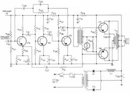
- Fig. 1b - Die Endstufe - (mit diversen Fehlern im Schaltplan) - beachten Sie den Koppeltransformator und den Ausgangstransformator

Only when the first ten objectives are achieved can preamplifier high fidelity be obtained.*) However, some deviation from the ideal may be permitted without serious impairment of the listening qualities of a system. The preamplifier design shown in Fig. 1 represents a good balance between performance and cost.
*) A loudness control may be desired following the observations of Fletcher and Munson. A discussion on loudness controls may be found in "Radio and TV News", April 1957, Vol. 57, No. 4, P. 42, "Why Loudness Control," N. H. Crowhurst.
Record Equalization
If a sine wave of given strength were to be recorded, the record could be made so that the lateral deviation of the cutting stylus would be independent of frequency variation. This method is called constant-amplitude recording.
However, at the high frequencies the playback needle would have to move so fast, that constant-amplitude recording is mechanically impractical. The same sine-wave signal could also be recorded at a decreasing amplitude as the frequency is increased.
In this manner, if the amplitude is reduced by one-half every time the frequency is doubled (6db per octave), the velocity of the needle would be independent of frequency. The disadvantage of this method (constant-velocity recording) is, that the amplitude at low frequencies would be so high that the needle would cross over into the adjacent track, while the amplitude at high frequencies would be so low, that very small scratches or plastic imperfections would lead to scratch noise. The obvious solution is to record at neither a constant amplitude nor a constant velocity, but a combination of both.
Too many "Standards" in the past
Not too many years ago, different manufacturers selected their own combinations of recording characteristics, and no one standard was widely adopted.
Presently, however, most American manufacturers employ the RIAA record characteristic shown in Fig. 2. This characteristic also
goes under the name RCA "New Orthophonic" and is identical to the new AES, the NARTB, and the EIA Standards.
The RIAA characteristic of the preamplifier
The preamplifier shown in Fig. 1 incorporates the necessary compensation to the RIAA characteristic. The compensation is provided by a feedback network consisting of R3, C12, and C13.
This network produces a high degree of feedback at the high frequencies, thus lowering the input impedance of the transistor. This use of a low input impedance with a crystal or ceramic pickup, which is contrary to normal concepts of crystal terminations is discussed in detail below.
Pickup Characteristic
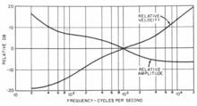
- Fig. 2 - Die RIAA Entzerrung

Ceramic and crystal pickups are basically amplitude-sensitive devices having an open-circuit output voltage directly proportional to the amplitude of the recorded signal. The relative-amplitude representation of the RIAA characteristic shown as "Curve B" is obtained by subtracting a six-db-per-octave curve from the relative-velocity presentation shown as "Curve A".
Most crystal and ceramic pickups have a controlled low-Q mechanical resonance at frequencies in the vicinity of 4 to 5 kilocycles. In this manner, an open-circuit output voltage which is somewhat flat with frequency may be obtained without equalization.
This system has many advantages in low-cost phonograph amplifiers utilizing high resistive loads (i.e., electron tubes).
Advantages in a transistor amplifier
In a transistor amplifier circuit, however, the output signal is a function of the input current. For good signal-to-noise ratio, therefore, the maximum current available should be used. Because the equivalent generator impedance of a ceramic or crystal pickup is capacitive (about 500-1300 micromicrofarads plus up to 200-300 micromicrofarads cable capacitance), the short-circuit current of the pickup is proportional to the velocity of the recorded signal.
If the mechanical resonance of the pickup has been carefully chosen and a minimum of equalization is desired, a single capacitor may be used for feedback from the collector to base of the transistor. The value of the capacitor is determined by the input resistance and gain of the transistor.
In the preamplifier shown in Fig. 1, the double-capacitor single-resistor network is used to provide better equalization.
Tone Controls
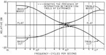
- Fig. 3 - Die Klangregelung

Individual adjustment of frequency response is provided by bass and treble cut or boost controls. Many preamplifiers rely upon tone-control functions for equalization. As a result, they have a very large range, particularly on bass boost.
When equalization is included in the design, tone controls covering a ±15db-to ±12db range at 100 cycles and 10 kilocycles are adequate. Separate tone controls should be such that provided for bass and treble.
Variation in the 1 kilocycle signal should not exceed ±1.5db for any position of the controls, and there should be very little interaction between the bass and treble.
Many boost circuits fix the frequencies to be boosted, and cut the other frequencies. This type of control is undesirable because it requires adjustment of the volume coincidental with the tone control. The method used for tone controls shown in Fig. 1 employs about 17db flat attenuation for each control, adding or subtracting attenuation selectively with frequency.
The large amount of high-frequency feedback used for equalization was employed rather than flat attenuation in the treble control circuit. Only about 6db total attenuation was used for the treble so that a considerable amount of equalization feedback is removed via loading in the treble boost position. This method permits less tone-control-insertion.
The tone control curves shown in Fig. 3 illustrate flat positions, extreme positions, and interaction. The degree of interaction is very slight for a tone-control network having such low insertion loss (23db total). It should be noted that neither ganged nor tapped pots entiometers are employed. Log-taper pots entiometers are desirable.
Pickup Resonances
- Fig. 4

The significance of pickup resonances was discussed previously. The pickup employed has a resonance of about 10 to 12db at frequencies of about 8 to 10 kilocycles. This resonance is compensated for by the network, R18, C18 as shown in Fig. 4.
Signal-to-Noise Ratio
The most obvious way to obtain a good signal-to-noise ratio is to use a strong signal. Crystal and ceramic pickups are known in the trade as high-output-level cartridges.
However, the largest output signal current from pickups is not necessarily obtained from the pickup having the largest open-circuit voltage because the short-circuit current is proportional to the open-circuit voltage times the pickup capacitance.
"High-level" cartridges which have a low value of capacitance may not be "high-level" output devices when used with transistor equipment in which the input signal is a current.
The signal-to-noise ratio of the preamplifier shown in Fig. 1 is of the order of 50db. Some of the noise is contributed by the second stage because of the attenuation caused by insertion of the tone controls.
Gain Adjustment
The location of the volume control in a transistor amplifier requires careful consideration. Improper location may shift the transistor bias conditions, increase the distortion, or degrade the frequency response as a function of the volume-control setting.
If the volume control is introduced too close to the input of the amplifier, the signal-to-noise ratio will be quite high at low level settings due to the noise of the stage after the control.
If the control is introduced too close to the output, however, the stage driving the volume control may overload. Considerable advantage may be gained if the volume control by feedback can be employed. Normally, however, the range of volume control obtainable by feedback is only in the order of 50db. This limitation would produce a serious problem of minimum gain setting.
Volume Control
A unique volume control is utilized in Fig. 1. As the gain is adjusted from the maximum to the minimum, the following conditions occur in the sequence shown with some degree of overlap.
.
- 1. The signal from the second transistor (V2) is attenuated due to series resistance.
- 2. The decreasing collector-to-base resistance introduces an increasing amount of third-stage feedback.
- 3. As the collector-to-base resistance continues to decrease, it loads down the third-stage collector.
- 4. As the collector-to-base resistance approaches the reciprocal of the transconductance (1/gm) of the third-stage transistor (V3), the feed-through approaches the collector output and complete cancellation is approached.
.
Some volume control is effected, therefore, by second-to-third-stage attenuation, some by third-stage feedback, some by third-stage-to-output attenuation, and some by cancellation. This arrangement overcomes some of the limitations described above pertaining to signal-to-noise ratio versus overload without the use of multiple potentiometers. The range of this control is of the order of 100 db.
Dynamic Range
The dynamic range of any amplifier stage may be expressed in db with the limits of operation bounded by noise at the low-level end and overload at the high-level end. Each stage must be analyzed separately for dynamic range in a circuit design to assure that the incoming signal under all conditions will be high enough to provide an adequate signal-to-noise ratio, yet low enough to avoid overloading. Because feedback extends the effective dynamic range, it is widely used wherever practical.
Considerations affecting dynamic range are as follows:
- 1. The Record Manufacturers use an average record velocity of 5.5 centimeters per second at 1 kilocycle. The average peak level is approximately 8db above this level. Some records are cut at lower velocities, however, to permit a greater peak range with some sacrifice in signal-to-scratch and signal-to-noise ratio. If equalization is accomplished prior to the first stage (or by feedback to the pickup around the first stage or stages), only an 8db range above the average velocity 5.5 centimeters per second plus any pickup resonances at 1 kilocycle need be considered. In the design shown in Fig. 1, the dynamic range of signal above average record level was about 18db (due to a 10db resonance of the pickup at 10 kilocycles) for the first stage, with a low-level range of about -6 db for low-level records.
- 2. The tone controls may be adjusted from about -12db to about +12db. This range results in a maximum signal level of about 30db above average, and a minimum of about -18db. The second stage must be capable, therefore, of handling a +30db signal without overload and a -18db signal with a tolerable signal-to-noise ratio.
- 3. If it is desirable to use a variety of pickups, the variation in signal level must also be considered.
- 4. Because the third stage incorporates the volume control in which volume is reduced about 50db either by feedback or by second-to-third-stage attenuation, this stage must be capable of delivering sufficient output at a -6db level to drive the power amplifier and sufficient signal at average level to overload the power amplifier without distortion. In addition, the signal-to-noise ratio at low volume setting must be tolerable.
.
Testing Precautions
Errors can arise during measurement of the frequency response of this preamplifier primarily because of the following reasons:
- 1. A slight degree of network interactions.
- 2. The use of current rather than voltage for reference in some circuit locations.
- 3. The capacitive generator offered by the pickup.
- 4. Pickup resonances.
- 5. RIAA equalization.
Although accurate evaluation of frequency response may be obtained by isolating the functions, this procedure requires a very thorough knowledge of the system.
Using an RIAA or RCA "New Orthophonic" test record
The most direct method for evaluating over-all performance is to include recording, turntable, and pickup performance. This test can be accomplished by monitoring the output voltage, using an RIAA or RCA "New Orthophonic" test record for the signal source. Amplifier Design Considerations
In the design of the power amplifier, the following objectives were considered:
.
- 1. It should provide a specified amount of power output, 10 watts, into a desired speaker impedance.
- 2. It should have a flat frequency response with low harmonic and intermodulation distortion.
- 3. It should provide sufficient gain so that the preamplifier can drive the power amplifier to rated output power.
- 4. It should operate from a relatively inexpensive power supply.
- 5. It should not require circuit adjustments when transistors are replaced.
- 6. It should have sufficient temperature stability to operate at ambient temperatures ranging from 0 to 55 degrees centigrade without serious degradation in performance or reliability.
.
Output Stage - class B operation
The output stage of the amplifier shown in Fig. 1 consists of two RCA "2&301" p-n-p germanium alloy-junction transistors operated in a class B push-pull circuit.
Class B operation is employed because it provides maximum efficiency and because the transistors can be biased essentially at cutoff to reduce standby power and minimize zero-signal dissipation. In most practical amplifier designs, a common-emitter or common-collector circuit configuration is used.
Although the common-emitter circuit provides the highest power gain, total harmonic distortion is usually higher than acceptable for the design of a high-quality audio amplifier.
The common-collector circuit results in lower distortion because of its inherent feedback, but it requires a considerable amount of driving power.
The class B output stage shown in Fig. 1 represents a combination of the common-emitter and common-collector circuits, and has a power gain which is intermediate between the two.
Amp with auto-transformer design
This output circuit employs an auto-transformer designed so that a portion of the winding can he connected in the emitter circuit to provide emitter degeneration and low harmonic distortion.
Because the dc resistance of the transformer windings is quite low, the dc power loss is minimized and a higher operating circuit efficiency results than would be obtained if resistors were inserted in the emitter circuit to provide the same degree of ac degeneration.
The output transformer is designed for use with a 16-ohm speaker, but can be modified easily to accommodate any desired speaker impedance. The output transformer incorporates bifilar windings to minimize leakage inductance and winding capacitance [1].
This method of winding provides approximately unity coupling between the two halves of the winding, and reduces transient voltages when current shifts from one output transistor to the other.
Temperature stabilization
Temperature stabilization for the class B output stage is provided by the network R43, R44 in the bias circuit. This network provides a compensating shift in bias with temperature variations which, in effect, causes the dc collector current to remain fairly constant. Because the collector junction of the power transistor is connected to the mounting flange, the flange must be electrically insulated from the chassis which is usually at ground potential.
At the same time, the mounting flange must make good thermal contact with the chassis. "Mica insulating washers" having a thickness of 0.002 inch are used to insulate the mounting flange electrically from the chassis. Because the mica washers have a high thermal conductance, the total circuit thermal resistance is not increased appreciably.
Driver Stage
The driver stage uses an RCA-2N301 power transistor in class A operation in the common-emitter circuit configuration. The output of the driver is transformer-coupled into the class B output stage. The primary winding of the driver transformer is wound between the secondary windings to minimize the effects of leakage inductance and winding capacitance [2]. The secondary winding consists fo four sections which are bifilar wound to provide tight coupling and thereby minimize transient voltages when current shifts from one output transistor to the other.
Anmerkung : Der Grundig SV50 von 1963 hatte auch noch die Transformator- Ankopplung der Endstufe an die Treiberstufe.
The source impedance presented to the input of the class B stage has a pronounced effect on the total harmonic distortion in the output stage. It has been shown previously [3] that the driving device should have a low output impedance to minimize distortion in the output stage.
The output impedance of the driver transistor is quite high and does not satisfy the condition for low distortion. The effective output impedance of this transistor is reduced by the use of shunt feedback from the collector to the base of the driver transistor. This arrangement, however, also causes a reduction in the effective input impedance of the driving device, and requires that the stage preceding the driver stage be operated as a power amplifier.
Pre-Driver and Input Stage
The pre-driver stage uses an RCA-2N270 low-power audio transistor in class A operation in the common-emitter circuit configuration. Because this stage operates into a low load impedance, it is designed as a power amplifier and is capacitively coupled to the driver input.
The bias voltage for this stage is determined by the voltage drops across R32, R33, and R34. The operating-point stability depends primarily on the emitter resistor R34 and the parallel combination of R32 and R33.
The input stage, which uses an RCA-2N109 low-power audio transistor, is designed as a class A common-emitter current amplifier. The bias voltage for the input stage is determined by the voltage drops across R27, R28, and (R30 + R31). The operating-point stability depends on the emitter resistors (R30 + R31) and the parallel combination of resistors R27 and R28. Application of negative feedback from the secondary of the driver transformer to the emitter of the input stage reduces the distortion and extends the frequency response of the three stages preceding the class B output stage.
Ripple voltage present at the secondary of the driver transformer causes hum to occur in the feedback path back to the emitter of the input stage. In order to "buck out" this source of hum, a second feedback loop which applies a ripple voltage in the opposite phase is connected from the primary of the driver transformer to the base of the input stage through C28 and R42. Capacitor C2n is used to prevent high-frequency instability.
Power Supply and Filtering
The power supply consists of a transformer, two silicon diodes, and a choke-input filter section. The power-supply transformer is designed to operate from normal line voltage (60 cycle, 117 volts ac) and supply 18 volts dc. The transformer is capable of delivering a maximum load current of 2 amperes.
Because the power supply is required to operate into a varying load impedance, a choke-input filter is used in conjunction with silicon diodes to provide good regulation. The choke, designed by the Hanna method [4], has an inductance of approximately 0.1 henry at a current of 1.5 amperes, with a dc resistance of approximately 0.5 ohm.
Performance
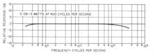
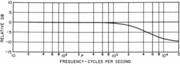
- Fig. 5 - The over-all frequency response

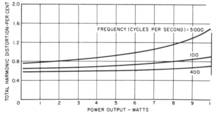
- Fig. 6 - The total harmonic distortion

The over-all frequency response of the transistorized power amplifier is shown in Fig. 5. The input voltage applied between the base of the input transistor and ground was kept constant during test. The frequency response is within 1db at frequencies from 30 to 15,000 cycles per second. Fig. 6 shows the variation in total harmonic distortion with power output for three different frequencies *).
At a power output of 10 watts, the total harmonic distortion is less than 1% for frequencies of 100 and 400 cycles per second. The distortion increases at 5 kilocycles because of the reduction in gain at high frequencies caused by transistor and transformer limitations **). Table I gives performance data for the power amplifier.
*) Measurements of frequency response and distortion were made in accordance with RMA Standard SE-101A.
**) For faithful reproduction the frequency response of a class I stage should be relatively flat to harmonics of the fundamental frequency. When only a few harmonics remain in the pass band o the output stage, distortion will result.
Table I - Power Amplifier Performance
Frequency Response 1db from 30- 15,000 cps at 3db down from rated P.O.
Power Output... 10.0 watts
Harmonic Distortion 1.0% at 10 watts and 400 cps
Intermodulation Distortion 3.0% ab 10 watts (60/3000 cps at 4:1)
Hum Level 57.5 db below rated power output
Maximum Ambient Temperature 55°C
.
- Anmerkung : Beachten Sie die maximale Umgebungstemperatur von 55°C - sogar in "Grad Celsius" angegeben - für die USA ist das sehr ungewöhnlich. Grund : Die ersten Germanium Transistoren waren damals noch extrem wärmeempfindlich.
.
References:
[1] F. Langford-Smith, "McIntosh Amplifier," Radiotron Designer's Handbook, Radio Corporation of America, Fourth Edition, p. 594.
[2] F. Langford-Smith, "Effects of Mixing Windings," Radiotron Designer's Handbook, Radio Corporation of America, pp. 221-222, Fourth Edition.
[3] R. Minton, "Class B Transistor Power Amplifier Design," Electronic Design, Vol. 5, No. 18, Sept. 15, 1957, pp. 24-27.
[4| F. Langford-Smith, "Design of Iron Core Inductors by Hanna Method," Radiotron Designer's Handbook, Radio Corporation of America, Fourth Edition, pp. 248-249.
addenda (wegen der diversen Fehler im Artikel oben) for
A Ten-Watt High-Quality Transistorized Audio Power Amplifer
In response to the numerous inquiries on the article, "A Ten-Watt High-Quality Transistorized Audio Power Amplifier" (see Feb. '58 SQ, p. 19), the authors have provided the following supplementary information:
Incidentally, the editors or SQ apologize for not doing this right the first time. Any "Boo-Boos" that slipped through were entirely ours. Sorry for the inconvenience. The authors were kind enough to help bail us out.
.
I. Circuit Corrections and Additions
The circuit diagram shown on page 20 should be amended as follows:
.
- A. The tie point at R20, R21, and C8 is erroneous. R21 should cross over to the base of V3.
- B. The short circuit between the center tap of the secondary of the driver transformer to ground should be removed.
- C. The following capacitors are electrolytics and the polarity is as designated below:
(1) C4, C31, and C32 should be connected with positive leads to ground.
(2) C27 and C28 have a voltage rating of 25 volts or greater. The positive leads of these capacitors are connected to V4. - D. The bias network for the Class B stage, located from the center tap of T1 to ground, is erroneously labeled. These two resistors should be labeled R45 (thermistor) and R46 as identified in the legend.
- E. When the preamplifier and power amplifier are used together, R24 should be 390 ohms.
II. Choke and Transformers
At the time of writing, the choke and transformer were not commercially available. In response to the interest developed in this amplifier, these components are now commercially available from
Columbus Process Company, Inc., 2851 Southeastern Ave., Columbus, Indiana.
.
Their part numbers are as follows:
- Driver Transformer (T1) #CPC3910
- Output Transformer (T2) #CPC3911
- Power Supply Transformer (T3) #CPC3912
- Power Supply Choke (L1) #CPC3913
III. Rectifiers
Any silicon power rectifier that is capable of 1 ampere rectified current and 50 volts peak inverse may be used for D1 and D2.
.